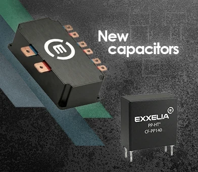
Exxelia introduces the CCM family at ESA / SPCD 2022

Magnetic components for space applications, optimized for multi output Flyback transformers


SUMMARY


  • Introduction : evolution of magnetic components in space

Definition – How to satisfy it?

  • Part 1 : Family qualification by ESA/CNES

Why choose Technology Flow over QPL products?

Qualification steps.

  • Part 2 : Performance characterization of CCM technology

Thermal behavior.

Frequency response and Current saturation (standard CCM inductors).

  • Part 3 : Optimization for multi output Flyback transformers

The cross regulation problem or voltage deviations on some outputs.

PhD thesis definition – Different stages of work – Present and future results.

  • Conclusion

Components that meet present and future customer needs


WHAT IS A CCM?


CCM family : INTRODUCTION


What are the new technical needs and constraints for specific transformers?


First : Applications with more outputs.

Need for more In/Out pins.

More different voltages and power levels.


Second : Increase in the power to volume and power to weight ratios.

We can no longer take large safety margins.

  →  need to know all the technical limitations of the product.

Reliability, internal heating, frequency response, current saturation.


Third : Development time is getting shorter

Breadboards/Prototypes must work the first time  →  design method must be accurate.

Even specific products must avoid qualification time.

  →  have to be already qualified before BreadBoard/Prototype step.


Part 1 : ESA qualification 


  • CCM family : What is this, and what is it for?

1 technology for 5 shapes

Ferrite circuit around windings wound in a bobbin, cabled on a leadframe and moulded.

For both standard and custom components

Different types of functions : inductors (DMC, CMC), pulse/SMPS/measurement transformers

  →  QPL qualification not adapted  Technology Flow is better


  • What is a Technology Flow?

Exxelia must prove that CCM technology is space compliant.

1st step Evaluation (Exxelia), 2d step Qualification (ESA/CNES).

Exxelia has to define : bill of materials / manufacturing process / design rules and list of tests to be performed.


Bill of materials

3 key raw materials : Bobbin, leadframe and magnetic circuit.

Other materials : wires, solid insulation, glue/resin/varnish, weld, ink, package.


Manufacturing process

3 key steps : winding, cabling, moulding.

Other steps : gluing, assembling, marking, testing, packaging.


Design rules

All theoretic actions the designer has to do upstream to prevent surprises downstream.


Test campaigns

All those in Charts F4 SG1, SG2 and SG3.

Thermal shocks, Temperature rise, Overload, Soldering heat, Vibrations, Mechanical shocks Operating life, Permanence of marking, Solderability, Terminal strength, Dielectric, Moisture.


  • Summary of work carried out

- More than 100 components designed, manufactured, and tested

  many configurations of  functions / shapes / tests.

- Some components destroyed to identify security margins

  on thermal, mechanical, dielectric aspects.

- Evaluation took several years to complete

 Result :  Qualification was successful on first try.


  • Conclusion

Respecting BOM, process and design rules qualified  ... Exxelia has the right to offer any function in CCM shapes without any mandatory testing for customer.


Part 2 : CCM technology performances


  • Security margins must be reduced

Maximum permissible loss value  →  leads to internal heating (Tmax <  125 °C).

Maximum operating frequency  →  above resonant frequency component is no more inductive.

Saturation curve  →  which inductor value at which excitation current?


  • How can these characteristics be determined ?

We decided to carry out 3 experimental campaigns :

  1. Thermal resistance determination for each of 5 shapes.
  2. Inductance versus frequency curves for standard inductors.
  3. Inductance versus current curves for standard inductors.


  • Thermal resistance Rth of CCM4, CCM5, CCM6, CCM20 and CCM25

  • Definition of test conditions

Use of inductors with one winding connected to all pins one side.


Measurements in vacuum are very complex.

  →  in natural convection in the air first.

Copper losses (heating source) only.

  →  DC current excitation / measurement of Rwind.

Component on PCB / all pins soldered  / no glue / no copper except for large current paths.

Component in a (pierced) box inside a ventilated oven  / temperature controlled.


  • Measurement bench

Measurements realised for each of 5 shapes.

2 L values  /  5 Tenv : 25, 50, 75, 100, 125 and 150°C  / up to 15 meas. points for each Tenv.


  • Complements and further work

Results applied for all CCM components  /  We have a math model air convection → vacuum.

3D simulations in progress to validate these curves  …  1st results are promising.

Measurements in vacuum are planned.


  • Frequency behavior for CCM4, CCM5, CCM6, CCM20 and CCM25 standard inductors


  • Definition of test conditions

Use of inductors with one winding connected to all pins one side.

Constant excitation, between 100µT and 1mT.

Components soldered on a brass plate.

RLC meter calibrated after 1 hour functioning.


Measurement device


  • Measurements realised for each of 5 shapes

2 L values  / up to 15 meas. points for each inductor value.


  • Result overview
    • Majority of inductors are usable at least up to 1MHz.
    • All of inductors are usable at least up to 400kHz.


  • Saturation behavior for CCM4, CCM5, CCM6, CCM20 and CCM25 standard inductors


  • Definition of test conditions

Use of inductors with one winding connected to all pins one side.

0,5 phase shift full bridge DC supply.

DC+AC (300kHz) excitation with duty cycle > 0,5.

ΔI constant as long as no saturation.

Period nb controlled to achieve desired DC current.

L value measured with current rise slope.


  • Measurements realised for each of 5 shapes

2 L values  / 2 Tenv, ambiant and 125°C / up to 15 meas. points for each Tenv.

2 types of curves L function of Idc or Imax (Idc+ΔI/2).


  • Result overview

Big ≠ between 25 and 125 °C : taking account of thermal behavior of ferrite is mandatory.

Main interest : to detect the beginning of saturation.


Part 3 : multi Flyback optimization


  • What are voltage deviations also named cross regulation problem ?
  1. At nominal point of load, some output voltages are different from theoretical values.
  2. If power level at regulated output varies, some non-regulated output voltages values vary.
  3. Current waveform on some auxiliary outputs is very different from theoretical triangle shape.


  • Observation :

The more different output / voltage levels / power levels …

The greater the probability to have voltage deviations.

Actual solution : linear regulators.

  →  more volume/weight, less efficiency, more heating.


  • Charge :  Transformer is mostly responsible

Problem seriousness depends on application and even on piece inside a manufacturing batch.

Magnetic root cause (transformer), but power electronics consequence (converter).

  →  need to work in both electromagnetism and power electronics.


  • Exxelia decided to manage a PhD thesis on this subject

Aims :

  1. Understand scientific problem, Identify root causes (transformer, other components?),
  2. Find solutions, Take account of voltage deviations in design and manufacturing process

Partners : G2Elab laboratory, D. Motte Michellon student, CNES, Steel Electronique


  • PhD step 1 : Understanding the scientific problem, identify root causes

Study of magnetic behavior of several transformers

  →  use of FLUX finite element simulation software

Identification of a circuit model compliant with several softwares (Psim, Spice, other)

  →  extended Cantilever magnetostatic model

Calculation of all output voltages for different transformers/converters

  →  use of Psim circuit software


  • Result of analysis :
  •  3/4 problem comes from transformer : magnetic coupling between all secondaries
  •  1/4 problem comes from drawbacks of some other components of converter


  • Actions :
  1.   Creating an analytic model to take account of leakage inductances between secondaries,
  2.   Use this model to quick calculate all output voltages.


  • PhD step 2 :  Finding theoretical and industrial solutions

We identified relationship between   CCM winding process, couplings between secondaries and voltage deviations.

We identified which other components and which drawbacks are concerned.

For the moment, one method of winding CCM to avoid worst cases of voltage deviations and to minimize variations from one piece to another applied since 01/01/2022 for all designed Flyback in CCM.

In progress, a software to optimize (minimize) voltage deviations and to identify best cases of CCM winding processes.

    →  Increase of know-how for customer benefit.


CCM family : CONCLUSION


  • Whatever the function you need

Component is already qualified  →  Reliability and security.

Many pins  ==  many input/output possibilities.

You know its thermal behavior  →  have a good idea of its energy/power limit.


  • For inductor applications

You can have standard or custom components.

You know frequency and current responses.


  • For multi output Flyback transformers

Design method focused on :

  1. meeting customer’s need as close as possible,
  2. volume and weight reductions.


Understanding voltage deviations  =  problem minimization + ability to assist customer.


                                                                CCM technology is well adapted for space   …  and we continue to improve it.


Autor : Bruno COGITORE  –  Jean PIERRE

Magnetic Expert / Innovation  –  Space product Manager  •  Exxelia Magnetics


Published on 05 Oct 2021 by Stephane PERES

What you should know about Ceramic Capacitors ?

▲ What you should know about Ceramic Capacitors ?   1. Materials expert For 50 years and as a market leader, EXXELIA’s comprehensive knowledge of the materials properties and performances have enabled us to design capacitors in Porcelain, NPO, BX, 2C1, BP, X7R and –2200ppm/°C ceramics. > See our capacitors in catalog   2. Custom Designs Our catalog products don’t meet your application?  Based on the valuable experience accumulated over the design of 2,000+ specific ceramic capacitors, you can trust EXXELIA to define a qualitative custom solution in a time effective manner.   3. No Obsolescence Choosing a standard or custom EXXELIA product means you won’t have to worry about obsolescence.   4. Typical Applications Aerospace & Defense: cockpit panels, flight control, radio systems, missile  guidance systems… Space: military and commercial satellites, launcher… Medical: MRI, external defibrillators, implantable devices… Telecommunications: base stations… Oil and gas: drilling tools, MWD, LWD, wellheads…   5. ISO 9001 And AS9100C Quality is at the core of Exxelia’s corporate culture. Each sites has its own certifications.    6. Certifications Capacitors manufactured by EXXELIA comply with American and European standards and meet the requirements of many international standards. For Space qualified parts (ESA QPL), please refer to our catalog «Ceramic capacitors for Space applications».   7. Quality & Reliability EXXELIA is committed to design and manufacture high quality and reliability products. The test cycles reproducing the most adverse operating conditions over extended periods (up to 10 000 hours) have logged to date well over 5.109 hours/°Component. Failure rate data can be provided upon request. 8. Conflict minerals EXXELIA is committed to an approach based on «Conflict Minerals Compliance». This US SEC rule demands complete traceability and a control mechanism for the mineral procurement chain, encouraging importers to buy only «certified» ore. We have discontinued relations with suppliers that procure from the Democratic Republic of the Congo or an adjoining country.   9. Environment EXXELIA is committed to applying a robust environmental policy, from product design through to shipment. To control its environmental footprint and reconcile this with the company’ functional imperatives, our environmental policy provides for the reduction or elimination of hazardous substances. We also focus on compliance with European Union directives and regulations, notably REACH and RoHS. 10. RoHS Compliancy SMD CAPACITORS The capacitor terminations are generally protected by a nickel barrier formed by electrolytic deposit. This barrier gives chip capacitors leaching performance far exceeding the requirements of all applicable standards. The nickel barrier guarantees a minimum resistance to soldering heat for a period of 1 minute at  260°C in a tin-lead (60/40) or tin-lead-silver (62/36/2) bath without noticeable alteration to the solderability. It also allows repeated soldering-unsoldering and the longer soldering times required by reflow techniques. However nickel barrier amplifies thermal shock and is not recommended for chip sizes equal or greater than CNC Y (30 30) - (C 282 to C 288 - CNC 80 to CNC 94). LEADED COMPONENTS As well as for SMD products, leaded capacitors ranges can also be RoHS. These products, which are characterized by the suffix «W» added to the commercial type, are naturally compatible with the soldering alloys used in RoHS mounting technology. The connections coating is generally an alloy SnAg (with a maximum of 4% Ag). However, on a few products that EXXELIA will precise on request, the coating is pure silver.   11. MLCC Structure   12. Equivalent circuit Capacitor is a complex component combining resistive, inductive and capacitive phenomena. A simplified schematic for the equivalent circuit is:   13. Dielectric characteristics  Insulation Resistance (IR) is the resistance measured under DC voltage across the terminals of the capacitor and consists principally of the parallel resistance shown in the equivalent circuit. As capacitance values and hence the area of dielectric increases, the IR decreases and hence the product (C x IR) is often specified in Ω.F or MΩ.µF. The Equivalent Series Resistance (ESR) is the sum of the resistive terms which generate heating when capacitor is used under AC voltage at a given frequency (f). Dissipation factor (DF) is the ration of the apparent power input will turn to heat in the capacitor: DF = 2π f C ESR When a capacitor works under AC voltage, heat power loss (P), expressed in Watt, is equal to: P = 2π f C Vrms2 DF   The series inductance (Ls) is due to the currents running through the electrodes. It can distort the operation of the capacitor at high frequency where the impedance (Z) is given as: Z = Rs + j (Ls.q - 1⁄(C.q)) with q = 2πf When frequency rises, the capacitive component of capacitors is gradually canceled up to the resonance frequency, where : Z = Rs and LsC.q2 = 1 Above this frequency the capacitor behaves like an inductor.   Manufacturing steps > See our capacitors in catalog SMD environmental tests Ceramic chip capacitors for SMD are designed to meet test requirements of CECC 32100 and NF C 93133 standards as specified below in compliance with NF C 20700 and IEC 68 standards: Solderability: NF C 20758, 260°C, bath 62/36/2. Adherence: 5N force. Vibration fatigue test: NF C 20706, 20 g, 10 Hz to 2,000 Hz, 12 cycles of 20 minutes each. Rapid temperature change: NF C 20714, –55°C to + 125°C, 5 cycles. Combined climatic test: IEC 68-2-38. Damp heat: NF C 20703, 93 %, H.R., 40°C. Endurance test: 1,000 hours, 1.5 URC, 125°C. > See our capacitors in catalog   STORAGE OF CHIP CAPACITORS TINNED OR NON TINNED CHIP CAPACITORS Storage must be in a dry environment at a temperature of 20°C with a relative humidity below 50 %, or preferably in a packaging enclosing a desiccant.  STORAGE IN INDUSTRIAL ENVIRONMENT: 2 years for tin dipped chip capacitors, 18 months for tin electroplated chip capacitors, 2 years for non tinned chip capacitors, 3 years for gold plated chip capacitors. STORAGE IN CONTROLLED NEUTRAL NITROGEN ENVIRONMENT: 4 years for tin dipped or electroplated chip capacitors, 4 years for non tinned chip capacitors, 5 years for gold plated chip capacitors. Storage duration should be considered from delivery date and not from batch manufacture date. The tests carried out at final acceptance stage (solderability, susceptibility to solder heat) enable to assess the compatibility to surface mounting of the chips.   LEAD STYLES   SOLDERING ADVICES FOR REFLOW SOLDERING   Large chips above size 2225 are not recommended to be mounted on epoxy board due to thermal expansion coefficient mismatch between ceramic capacitor and epoxy. Where larger sizes are required, it is recommended to use components with ribbon or other adapted leads so as to absorb thermo-mechanical strains. RECOMMENDED FOOTPRINT FOR SMD CAPACITORS  Ceramic is by nature a material which is sensitive both thermally and mechanically. Stresses caused by the physical and thermal properties of the capacitors, substrates and solders are attenuated by the leads. Wave soldering is unsuitable for sizes larger than 2220 and for the higher ends of capacitance ranges due to possible thermal shock (capacitance values given upon request). Infrared and vapor phase reflow, are preferred for high reliability applications as inherent thermo-mechanical strains are lower than those inherent to wave soldering.    SOLDERING ADVICES FOR IRON SOLDERING Attachment with a soldering iron is discouraged due to ceramic brittleness and the process control limitations. In the event that a soldering iron must be used, the following precautions should be observed: Use a substrate with chip footprints big enough to allow putting side by side one end of the capacitor and the iron tip without any contact between this tip and the component, place the capacitor on this footprint, heat the substrate until the capacitor’s temperature reaches 150°C minimum (preheating step, maximum 1°C per second), place the hot iron tip (a flat tip is preferred) on the footprint without, touching the capacitor. Use a regulated iron with a 30 watts maximum, power. The recommended temperature of the iron is 270 ±10°C. The temperature gap between the capacitor and the iron tip must not exceed 120°C, leave the tip on the footprint for a few seconds in order to increase locally the footprint’s temperature, use a cored wire solder and put it down on the iron tip. In a preferred way use Sn/Pb/Ag 62/36/2 alloy, wait until the solder fillet is formed on the capacitor’s termination, take away iron and wire solder, wait a few minutes so that the substrate and capacitor come back down to the preheating temperature, solder the second termination using the same procedure as the first, let the soldered component cool down slowly to avoid any thermal shock.   14. Packaging TAPE AND REEL The films used on the reels correspond to standard IEC 60286-3. Films are delivered on reels in compliance with document IEC 286-3 dated 1991. Minimum quantity is 250 chips. Maximum quantities per reel are as follows: Super 8 reel - Ø 180: 2,500 chips. Super 8 reel - Ø 330: 10,000 chips. Super 12 reel - Ø 180: 1,000 chips. Reel marking complies with CECC 32100 standard: Model. Rated capacitance. Capacitance tolerance. Rated voltage. Batch number.   15. Dimensional characteristics of chips tray packages   16. High Q Capacitors Tape and Reel Packaging Specifications   17. EIA standard capacitance values Following EIA standard, the values and multiples that are indicated in the chart below can be ordered. E48, E96 series and intermediary values are available upon request.   18. EIA capacitance code The capacitance is expressed in three digit codes and in units of pico Farads (pF). The first and second digits are significant figures of the capacitance value and the third digit identifies the multiplier. For capacitance value < 10pF, R designates a decimal point.  See examples below:   19. Part marking voltage codes Use the following voltage code chart for part markings: 20. Part marking Tolerance codes Use the following tolerance code chart for part markings:   21. Reliability levels Exxelia proposes different reliability levels for the ceramic capacitors for both NPO and X7R ceramics.   As the world’s leading manufacturer of specific passive components, we stand apart through our ability to quickly evaluate the application specific engineering challenges and provide a cost-effective and efficient solutions. For requirements that cannot be met by catalog products, we offer leading edge solutions in custom configuration: custom geometries, packaging, characteristics, all is possible thanks to our extensive experience and robust development process, while maintaining the highest level of reliability. Where necessary, special testing is done to verify requirements, such as low dielectric absorption, ultra-high insulation resistance, low dissipation factor, stability under temperature cycling or under specified environmental conditions, etc. > See our capacitors in catalog