Exxelia introduces the CCM family at ESA / SPCD 2022
Magnetic components for space applications, optimized for multi output Flyback transformers
SUMMARY
- Introduction : evolution of magnetic components in space
Definition – How to satisfy it?
- Part 1 : Family qualification by ESA/CNES
Why choose Technology Flow over QPL products?
Qualification steps.
- Part 2 : Performance characterization of CCM technology
Thermal behavior.
Frequency response and Current saturation (standard CCM inductors).
- Part 3 : Optimization for multi output Flyback transformers
The cross regulation problem or voltage deviations on some outputs.
PhD thesis definition – Different stages of work – Present and future results.
- Conclusion
Components that meet present and future customer needs
WHAT IS A CCM?
CCM family : INTRODUCTION
What are the new technical needs and constraints for specific transformers?
First : Applications with more outputs.
Need for more In/Out pins.
More different voltages and power levels.
Second : Increase in the power to volume and power to weight ratios.
We can no longer take large safety margins.
→ need to know all the technical limitations of the product.
Reliability, internal heating, frequency response, current saturation.
Third : Development time is getting shorter
Breadboards/Prototypes must work the first time → design method must be accurate.
Even specific products must avoid qualification time.
→ have to be already qualified before BreadBoard/Prototype step.
Part 1 : ESA qualification
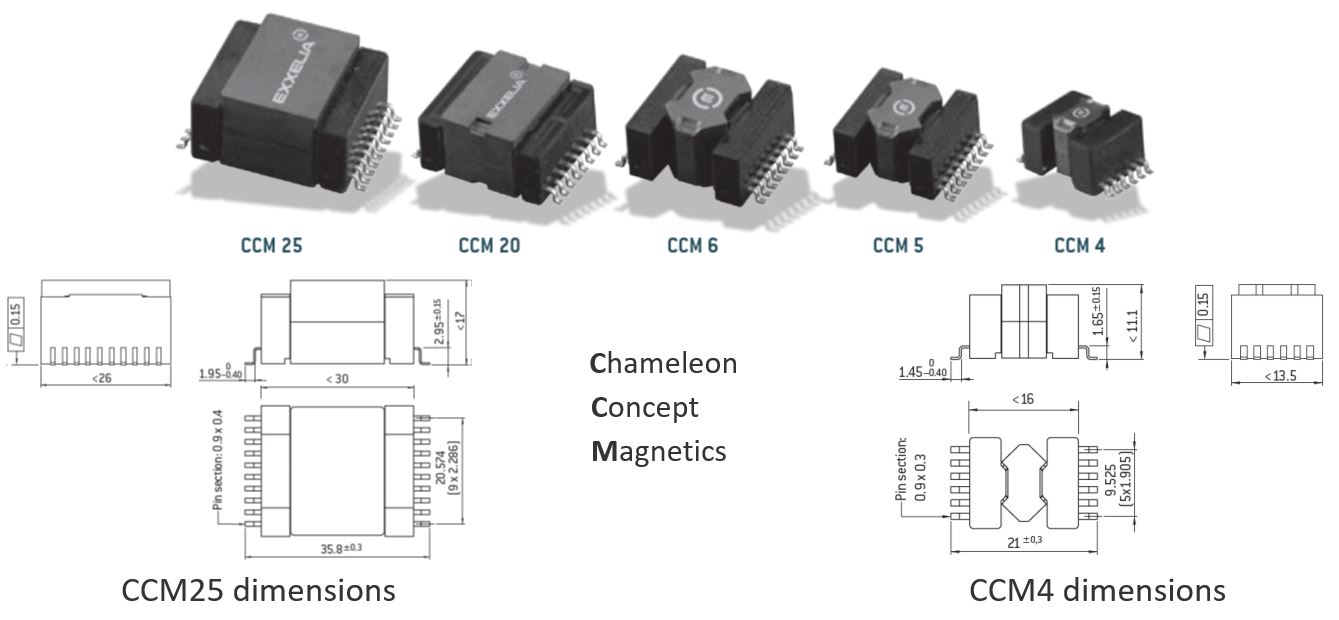
- CCM family : What is this, and what is it for?
1 technology for 5 shapes
Ferrite circuit around windings wound in a bobbin, cabled on a leadframe and moulded.
For both standard and custom components
Different types of functions : inductors (DMC, CMC), pulse/SMPS/measurement transformers
→ QPL qualification not adapted Technology Flow is better
- What is a Technology Flow?
Exxelia must prove that CCM technology is space compliant.
1st step Evaluation (Exxelia), 2d step Qualification (ESA/CNES).
Exxelia has to define : bill of materials / manufacturing process / design rules and list of tests to be performed.
Bill of materials
3 key raw materials : Bobbin, leadframe and magnetic circuit.
Other materials : wires, solid insulation, glue/resin/varnish, weld, ink, package.
Manufacturing process
3 key steps : winding, cabling, moulding.
Other steps : gluing, assembling, marking, testing, packaging.
Design rules
All theoretic actions the designer has to do upstream to prevent surprises downstream.
Test campaigns
All those in Charts F4 SG1, SG2 and SG3.
Thermal shocks, Temperature rise, Overload, Soldering heat, Vibrations, Mechanical shocks Operating life, Permanence of marking, Solderability, Terminal strength, Dielectric, Moisture.
- Summary of work carried out
- More than 100 components designed, manufactured, and tested
many configurations of functions / shapes / tests.
- Some components destroyed to identify security margins
on thermal, mechanical, dielectric aspects.
- Evaluation took several years to complete
Result : Qualification was successful on first try.
- Conclusion
Respecting BOM, process and design rules qualified ... Exxelia has the right to offer any function in CCM shapes without any mandatory testing for customer.
Part 2 : CCM technology performances
- Security margins must be reduced
Maximum permissible loss value → leads to internal heating (Tmax < 125 °C).
Maximum operating frequency → above resonant frequency component is no more inductive.
Saturation curve → which inductor value at which excitation current?
- How can these characteristics be determined ?
We decided to carry out 3 experimental campaigns :
- Thermal resistance determination for each of 5 shapes.
- Inductance versus frequency curves for standard inductors.
- Inductance versus current curves for standard inductors.
- Thermal resistance Rth of CCM4, CCM5, CCM6, CCM20 and CCM25
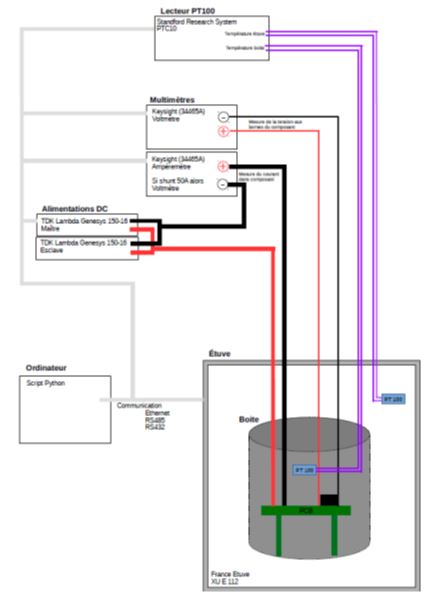
- Definition of test conditions
Use of inductors with one winding connected to all pins one side.
Measurements in vacuum are very complex.
→ in natural convection in the air first.
Copper losses (heating source) only.
→ DC current excitation / measurement of Rwind.
Component on PCB / all pins soldered / no glue / no copper except for large current paths.
Component in a (pierced) box inside a ventilated oven / temperature controlled.
- Measurement bench
Measurements realised for each of 5 shapes.
2 L values / 5 Tenv : 25, 50, 75, 100, 125 and 150°C / up to 15 meas. points for each Tenv.
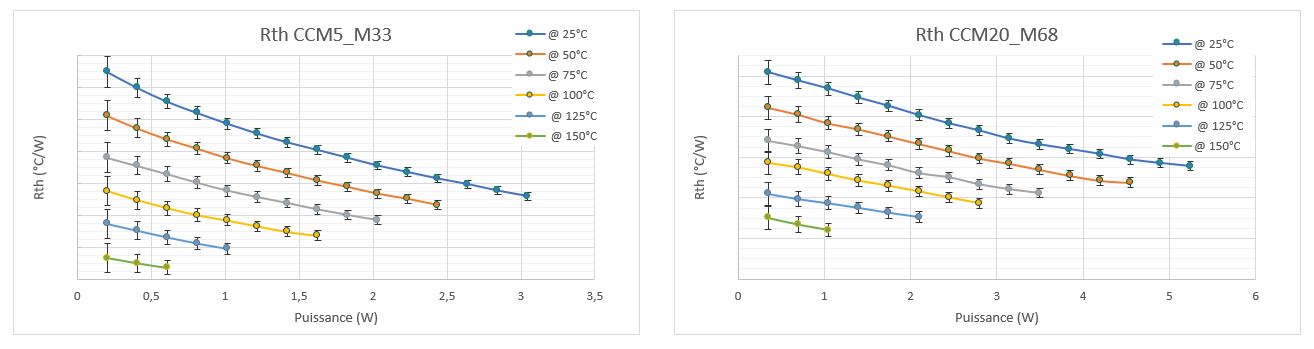
- Complements and further work
Results applied for all CCM components / We have a math model air convection → vacuum.
3D simulations in progress to validate these curves … 1st results are promising.
Measurements in vacuum are planned.
- Frequency behavior for CCM4, CCM5, CCM6, CCM20 and CCM25 standard inductors
- Definition of test conditions
Use of inductors with one winding connected to all pins one side.
Constant excitation, between 100µT and 1mT.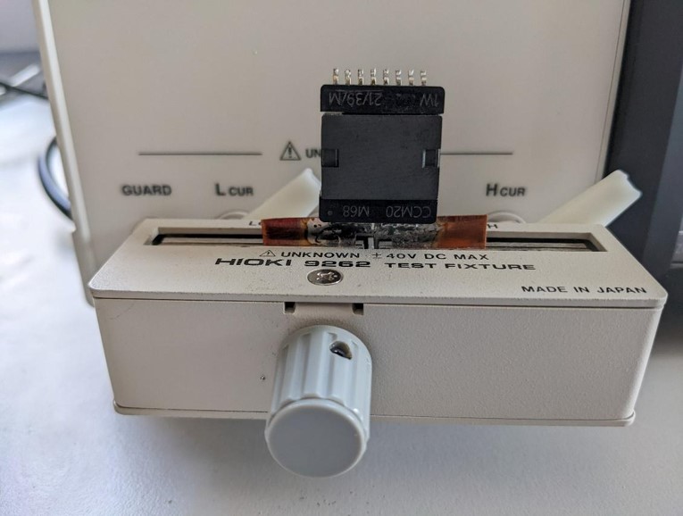
Components soldered on a brass plate.
RLC meter calibrated after 1 hour functioning.
Measurement device
- Measurements realised for each of 5 shapes
2 L values / up to 15 meas. points for each inductor value.
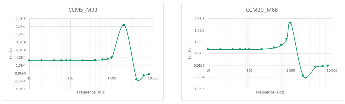
- Result overview
- Majority of inductors are usable at least up to 1MHz.
- All of inductors are usable at least up to 400kHz.
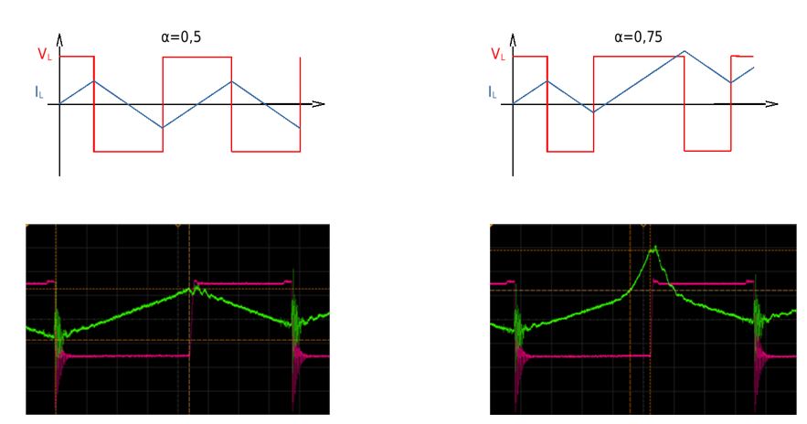
- Saturation behavior for CCM4, CCM5, CCM6, CCM20 and CCM25 standard inductors
- Definition of test conditions
Use of inductors with one winding connected to all pins one side.
0,5 phase shift full bridge DC supply.
DC+AC (300kHz) excitation with duty cycle > 0,5.
ΔI constant as long as no saturation.
Period nb controlled to achieve desired DC current.
L value measured with current rise slope.
- Measurements realised for each of 5 shapes
2 L values / 2 Tenv, ambiant and 125°C / up to 15 meas. points for each Tenv.
2 types of curves L function of Idc or Imax (Idc+ΔI/2).

- Result overview
Big ≠ between 25 and 125 °C : taking account of thermal behavior of ferrite is mandatory.
Main interest : to detect the beginning of saturation.
Part 3 : multi Flyback optimization
- What are voltage deviations also named cross regulation problem ?
- At nominal point of load, some output voltages are different from theoretical values.
- If power level at regulated output varies, some non-regulated output voltages values vary.
- Current waveform on some auxiliary outputs is very different from theoretical triangle shape.
- Observation :
The more different output / voltage levels / power levels …
The greater the probability to have voltage deviations.
Actual solution : linear regulators.
→ more volume/weight, less efficiency, more heating.
- Charge : Transformer is mostly responsible
Problem seriousness depends on application and even on piece inside a manufacturing batch.
Magnetic root cause (transformer), but power electronics consequence (converter).
→ need to work in both electromagnetism and power electronics.
- Exxelia decided to manage a PhD thesis on this subject
Aims :
- Understand scientific problem, Identify root causes (transformer, other components?),
- Find solutions, Take account of voltage deviations in design and manufacturing process
Partners : G2Elab laboratory, D. Motte Michellon student, CNES, Steel Electronique

- PhD step 1 : Understanding the scientific problem, identify root causes
Study of magnetic behavior of several transformers
→ use of FLUX finite element simulation software
Identification of a circuit model compliant with several softwares (Psim, Spice, other)
→ extended Cantilever magnetostatic model
Calculation of all output voltages for different transformers/converters
→ use of Psim circuit software
- Result of analysis :
- 3/4 problem comes from transformer : magnetic coupling between all secondaries
- 1/4 problem comes from drawbacks of some other components of converter
- Actions :
- Creating an analytic model to take account of leakage inductances between secondaries,
- Use this model to quick calculate all output voltages.
- PhD step 2 : Finding theoretical and industrial solutions
We identified relationship between CCM winding process, couplings between secondaries and voltage deviations.
We identified which other components and which drawbacks are concerned.
For the moment, one method of winding CCM to avoid worst cases of voltage deviations and to minimize variations from one piece to another applied since 01/01/2022 for all designed Flyback in CCM.
In progress, a software to optimize (minimize) voltage deviations and to identify best cases of CCM winding processes.
→ Increase of know-how for customer benefit.
CCM family : CONCLUSION
- Whatever the function you need
Component is already qualified → Reliability and security.
Many pins == many input/output possibilities.
You know its thermal behavior → have a good idea of its energy/power limit.
- For inductor applications
You can have standard or custom components.
You know frequency and current responses.
- For multi output Flyback transformers
Design method focused on :
- meeting customer’s need as close as possible,
- volume and weight reductions.
Understanding voltage deviations = problem minimization + ability to assist customer.
CCM technology is well adapted for space … and we continue to improve it.
Autor : Bruno COGITORE – Jean PIERRE
Magnetic Expert / Innovation – Space product Manager • Exxelia Magnetics